

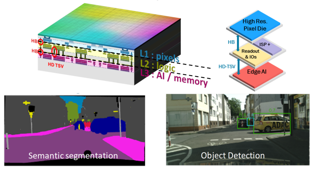
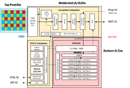
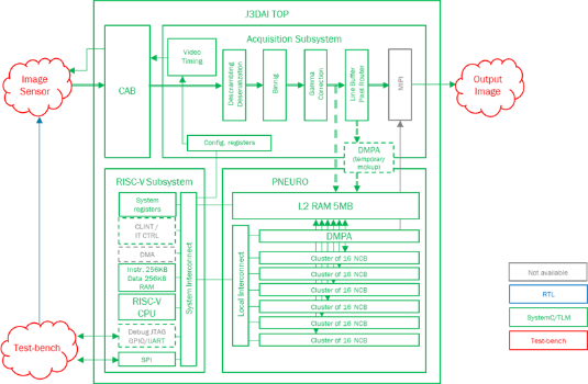
A smart imager architecture based on a new three-layer integration was developed for the IRT Smart Imager program. The chip, called J3DAI, integrates CEA-List’s PNeuro hardware accelerator, which enables inference learning by several AI networks at the imager level.
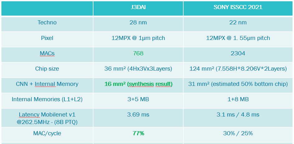
The architecture developed (Figure 1) required 50 mW of power for a video stream of 30 frames per second in tests on a Mobilenet V1-type network. In addition, a performance and area comparison with Sony’s AI imager published in 2021 at the ISSCC conference showed similar execution times (3.69 ms vs. 3.1 ms) but with three times fewer MACs (multiply-cumulate operations) at 768 vs. 2304, and three times less silicon area (36 mm² vs. 124 mm²) as shown in the table in Figure 2.
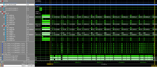
A virtual platform (Figure 4) was also developed using Siemens CAD tools. Based on a PNeuro system and RISC-V (32-bit) processor, the platform enables significantly faster simulation (2,000 times faster at 13 seconds vs. 7h and 45 minutes) of complex tasks, with results comparable to those produced using low-level simulation.
Smartphones—once a key market for image sensors—are seeing much slower growth. Image sensors are adapting to address the automotive, industrial, and security markets, where new opportunities are being created. The multi-layer 3D integrations developed for the Smart Imager program enable embedded AI on the same chip as the sensor, responding effectively to the current and future market challenges faced by the program’s partner companies.
improvement in MAC efficiency and silicon surface area
A smart imager for intensive real-time image analysis